LOOKING FOR XILINX FPGA BOARDS

Verilog Course Team is now authorized distributor for Digilent-Xilinx FPGA Boards, For more details visit www.verilogcourseteam.com/products or Contact @ +91 9894220795.

Wednesday, July 23, 2008

Verilog Coding Guidelines- Part 5

5. FILE STRUCTURE

5.1 One file, one module

Create separate files for each modules. Name the file .v. The only exceptions for this
file naming convention shall be the technology-dependent modules (top module or macro
wrapper modules). These files shall be appropriately named like design_name_fpga.v, design_name_tsmc.v, or design_name_virtex.v.

5.2 File header

Each source file should contain a header at the top of the file in the following
format:
/////////////////////////////////////////////////////////////////
//////////
//(c) Copyright 2008 Verilog Course Team/Company Name. All rights reserved
//
// File:
// Project:
// Purpose:
// Author:
//
// $Id: index.html,v 1.1 2008/0773/23 01:55:57 VCT $
//
// Detailed description of the module included in the file.
//Include relevant part of the spec
// Logical hierarchy tree
// Block diagrams
// Timing diagrams etc.
//
/////////////////////////////////////////////////////////////////

The above example is for verilog. Change the comment characters appropriately for other source types. Example: "#" in Tcl, Perl and CSH. The presence of variable $Id$ in the header will capture the filename, user, version information every time the file is checked-in/committed.

5.3 Modification history

Each file should contain a log section at the bottom of the file in the following format:
///////////////////////////////////////////////////////////////////////
////
//
// Modification History:
//
// $Log$
//
///////////////////////////////////////////////////////////////////////

Listing the modification history at the top of the file can be annoying as one has to scroll down to reach the code every time the file is opened for reading. The variable $Log$ will cause RCS/CVS to capture the user-comments entered during each check-in/commit as comments in footer section.

5.4 Include Files

Keep the `define statements and Parameters for a design in a single separate file and name the file DesignName_params.v

Verilog Coding Guidelines - Part 4

4. DO’S AND DONT’S

4.1Use non-blocking assignments in sequential blocks

All registers assignments are concurrent. No combinatorial logic is allowed in sequential blocks. Always use non-blocking statements here.

4.2 Use blocking assignments in combinational blocks

Concurrency is not needed here. Often the combinatorial logic is implemented in multiple steps. Always use blocking statements for combinatorial blocks.

4.3 Ensure that there are no unused signals

Unused signals in the designs are often clear indication of incomplete or erroneous design. Check to make sure that design does not contain such signals.

4.3 Ensure that there are no un-driven signals

Un-driven signals in the designs are mostly clear indication of design errors. Check to make sure that design does not contain such signals.

Verilgo Coding Guidelines -Part 3

3. COMMENT

3.1 Comment blocks vs scattered comments

Describe a group of logic at the beginning of the file (in the header) or at the top of a block or group of blocks. Avoid scattering the comment for a related logic. Typically the reader would like to go through the comment and then understand the code itself. Scattered comment can make this exercise more tedious.

Example:

//File:
//purpose:
//Project:
//Author:

3.2 Meaningful comments

Do not include what is obvious in the code in your comments. The comment should typically cover what is not expressed through the code itself.

Example:

History of a particular implementation, why a particular signal is used, any
algorithm being implemented etc.

3.3 Single line comments

Use single line comments where ever possible. i.e. Use comments starting with ’//’ rather than ’/* .. */’ style. This makes it easy to cut-paste or move around the code and comments. It is also easy to follow the indentation with single line comments which makes the code more readable.


Verilog Coding Guidelines -Part 2

2. STYLE

2.1 Page width: 75 characters

Considering the limited page width supported in many terminals and printers, restrict the maximum line length to 75 characters. For reuse macros reduce this number to 72 to comply with RMM.

2.2 No tabs

Do not use tabs for indentation. Tab settings are different in different environments and hence can spoil the indentation in some setup.

2.3 Port ordering

Arrange the port list and declarations in a cause and effect order. Group the list/declaration on the basis of functionality rather than port direction etc. Specify the reset and clock signals at the top of the list.

2.4 One statement per line

Limit the number of HDL statements per line to one. Do not include multiple statements, separated by semicolon, in the same line. This will improve readability and will make it is easy to process the code using scripts and utilities.

2.5 One declaration per line

Limit the number of port, wire or reg declaration per line to one. Do not include multiple declarations, separated by commas, in the same line. This will make it easy to comment, add, or delete the declared objects.

Example:

Wrong way:
input trdy_n, stop_n;

Right way:
input trdy_n;
input stop_n;

Wednesday, July 16, 2008

Verilog Coding Guidelines -Part 1

1. Naming Conventions

1.1 Character set


Use only the characters [a-z][A-Z][0-9] $ and "_" in the identifiers used for naming module, ports, wires, regs, blocks etc.

Do not use escaped identifiers to include special characters in identifiers. Do not use the character "_" as the first or last character of an identifier. Do not use numerals as first character.

Do not use capital letters for identifier except Parameter and define

Example:conventions.v

1.2 Case sensitive

Use lower case letters for all identifiers leaving the upper case letters for macros and parameters. Do not use the mixed case style. Also, ensure that all the identifiers in the design are unique even in a case insensitive environment.

Example:

module // keyword Module // unique identifier but not keyword

MODULE // unique identifier but not keyword Identifier

Name: fifoReadPointer.
Use: fifo_read_pointer- instead.

1.3 No keywords

Do not use Verilog keywords as identifiers.
Avoid keywords from both the HDLs as RTL code of a re-usable design may have to be made available in both languages.

Example:

input –keyword

output –keyword

1.4 Use meaningful Names

Create identifiers by concatenating meaningful words or commonly used acronyms separated by character "_".

Example:

Use en_state_transition instead of est or en_st_trn.

1.5 Identifier length, and number of parameters

Do not to use very long identifiers. This is especially true for parameters. Design unit names of parameterized modules are created by concatenating instance names, values and parameter names during design elaboration. Limit the maximum number of characters in an identifier to 25.

1.6 Parameter/Define naming convention

Parameter and Define must be declared in Capital Letter.

Example:

Parameter DATA_WIDTH=3’b111 ; `define EXAMPLE

1.7 Module names

Name the top level module of the design as _top. Module name & file name must be identical This is typically the module containing IO buffers and other technology- dependent components in addition to module _core. Module _core should contain only technology independent portion of the design. Name the modules created as macro wrappers _wrap.

Example:

module test (port1,port2,…);
.............
.............
.............
endmodule

The file should be saved as test.v

1.8 Instance names

If the module has single instance in that scope use inst_ as instance name. If there are more than one instance, then add meaningful suffixes to uniquify the names. Remember that the instance name in gate level netlist is a concatenation of RTL instance name and all the parameter ids and values in the instantiated module.

• A module may be instantiated within another module
• There may be multiple instances of the same module
• Ports are either by order or by name
• Use by order unless there are lots of ports
• Can not mix the two syntax's in one instantiation
• Always use module name as instance name.

Example:

memory memory_instance

syntax for instantiation with port order:
module_name instance_name (signal, signal...);

syntax for instantiation with port name:
module_name instance_name (.port_name(signal), .port_name (signal)… );

1.9 Blocks names

Label all the always blocks in the RTL code with meaningful names. This will be very useful for grouping/ungrouping of the design in synthesis tool and will result in better error/info messages. It is a standard practice to append the block labels with "_comb" or "_seq" depending on whether it is combinatorial or sequential.

Example:


1.10 Global signals

Keep same names for global signals (rst, clk etc.) in all the hierarchies of the design.
This should be true for any signal which are used in multiple design hierarchies. The actuals and formals in instantiation port maps should be the same IDs.

1.11 Clock signals

Name the clock signal as clk if there is only one clock in the design. In case of multiple clocks, use _clk as suffix.

Example:

pci_clk, vci_clk.

Never include the clock frequecy in clock signal name (40MHz_clk) since clock frequencies often change in the middle of the design cycle.

1.12 Reset signals

Name the reset signal as rst if there is only one reset in the design. In case of multiple resets, use _rst as suffix.

Example:

pci_rst, vci_rst.


1.13 Active low signals

All signals are lowercase alpha, numeric and underscore only. Use _n as suffix.

Example:

intr_n, rst_n, irdy_n.

Avoid using characters ’#’ or ’N’ as suffixes even in documents.

1.14 Module Hierarchy

A hierarchical path in Verilog is in form of:

module_name.instance_name.instance_name

top.a.b.c is the path for the hierarchy below.

1.15 Use of Macros

Macros are required to be used for any non-trivial constants, and for all bit-ranges. This rule is essential both for readability and maintainability of code. Having two inter-connected modules, each of which defines a bus as '17:0' is a recipe for disaster. Busses are preferably defined with a scheme such as the following:

`define BUS_MSB 17

`define BUS_LSB 0

`define BUS_SIZE (`BUS_MSB-`BUS_LSB+1)

`define BUS_RANGE `BUS_MSB:`BUS_LSB

This will minimize the number of places that have to be changed if the bus size must be changed.

1.16 MEMORY DECLARTION

Memories are declared as two-dimensional arrays of registers.

syntax: reg [msb:lsb] identifier [first_addr:last_addr] ;

where msb:lsb determine the width (word size) of the memory first_addr:last_addr determine the depth (address range) of the memory

1.17 Abbreviation

Use consistent abbreviation as shown:

Signal Naming Abbreviation

Tuesday, July 15, 2008

Verilog 8

1. How to generate random number in Verilog.


2.Is this code is synthesizable?
always@(negedge clk or rst)

3.What is a code coverage and list the types.

4. How to swap 2 variables A and B without using 3 variable.

5. Write Verilog Code to generate 80 MHZ clock with 50% duty cycle.

Thursday, July 10, 2008

Verilog 7

Consider the following code,
always@(posedge clk)
begin
a=b;
b=c;
c=a;
end
What logic does the code implies.

Synthesis 1


What will be the synthesis structure?

Digital 4

Design EX‐OR gate using 4 NAND gates.

Design EX‐NOR gate using 4 NOR gates.

General 1

What are the parameters to be considered before starting the design work.

Verilog 6

What is the advantage of using Gray code instead of Binary code while designing FIFO.
Write the Verilog Code for the Binary to Gray and Gray to Binary.

Verilog 5

How to test the functionality (test cases) of a FIFO.
Write the Verilog Code for the same.

Verilog 4

Consider the following code:
always@(posedge clk)
if(rst==0)
out<=1’b0;
else
out<=data_in;
a. Draw the synthesis view for the above code.
b. Modify the code for Asynchronous Reset.
c. Draw the timing diagram for synchronous and asynchronous reset.

Digital 3

Draw the circuit to avoid the Set‐up and Hold‐time violation.

Digital 2

Design AND, OR gate using 2:1 mux.

Verilog 3

Consider the following code:
`define FALSE 0
`define TRUE 1
initial
begin
a = `FALSE;
a <= `TRUE;
if (a == `TRUE)
$display ("True");
else
$display ("False");
end
What will print out? True or False?

Verilog 2


After the first @ (posedge clk), does this do a swap?

Verilog 1


Assume b = 3 and c = 5, after the first @ (posedge clk) what is the value of a?

Digital 1


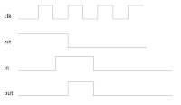
Design a circuit(positive edge ) that detect the sequence when input changes from 0 to 1,the output should go high for only one clock pulse.

DISCLAIMER

Verilog Course Team does not warrant or assume any legal liability or responsibility for the accuracy, completeness, or usefulness of any information, apparatus, product, or process disclosed. No warranty of any kind, implied, expressed or statutory, including to fitness for a particular purpose and freedom from computer virus, is given with respect to the contents of this blog or its hyper links to other Internet resources. Reference in this blog to any specific commercial products, processes, or services, or the use of any trade, firm or corporation name is for the information, and does not constitute endorsement, recommendation, or favoring.